
Titanium (Ti) Sputtering Target — Industrial 2N7 to Semiconductor 5N Purity for PVD Thin Film Deposition
Ti (Titanium) sputtering target is a widely‑used refractory metal consumable for magnetron PVD sputtering. Known for good corrosion resistance, high melting point and excellent film uniformity, titanium targets produce reliable adhesive thin films for semiconductor, optics, medical device and decorative coating industries. We supply 3N‑5N high‑purity Ti sputtering targets in disc, plate and custom geometries. Full test documentation including COA is provided for industrial manufacturers and research labs. Bonding service, custom dimensions and bulk order support are available. Contact us for detailed specifications and competitive bulk pricing.
Technical Specifications
| Parameter | Value |
|---|---|
| Product | Titanium (Ti) Sputtering Target — Planar, Rotary & Bonded Assemblies for PVD Thin Film Deposition |
| Chemical Symbol | Ti | Atomic Number: 22 | CAS: 7440-32-6 |
| Purity Grades | Industrial Grade: 99.7% (2N7) | High Purity: 99.99% (4N) | Ultra-High Purity: 99.999% (5N) |
| Density | 4.506 g/cm³ (theoretical) | Typical target density: ≥99.5% theoretical |
| Melting Point | 1,668 °C |
| Grain Size | <20 μm (industrial grade) | <50 μm (high purity grade) — finer grain on request |
| Key Properties | High strength-to-weight ratio, low density, ductile (especially in oxygen-free environment), metallic-white lustrous, paramagnetic, low electrical and thermal conductivity, excellent corrosion resistance, refractory |
| Target Forms | Planar (round, rectangular), rotary targets/arc cathodes, bonded to Cu backing plates |
| Manufacturing Process | Vacuum Melting → Forging → Rolling → Annealing → Machining → Final Inspection → Packaging |
Product Overview
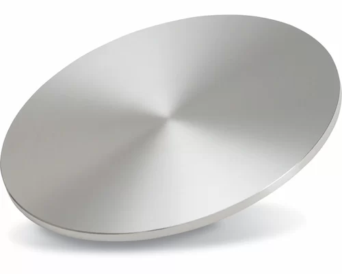
Titanium (Ti) sputtering targets are high-performance consumable cathode materials used in physical vapor deposition (PVD) processes — including DC/RF magnetron sputtering, reactive sputtering, and arc evaporation — to deposit thin titanium films and titanium-based compound coatings (TiN, TiC, TiCN, TiO2) onto substrates spanning semiconductor wafers, architectural glass, luxury goods, optical lenses, and flat panel displays. Princeton Powder supplies titanium sputtering targets in three purity grades — 99.7% (2N7) industrial, 99.99% (4N) high purity, and 99.999% (5N) ultra-high purity — manufactured through vacuum melting, forging, rolling, and precision machining to deliver consistent sputtering performance, uniform erosion profiles, and minimal particle generation.
Titanium is the world's most widely sputtered metal for decorative PVD coatings: when reactively sputtered in a nitrogen-containing atmosphere, titanium forms titanium nitride (TiN) — a brilliant golden-yellow ceramic coating with hardness exceeding 20 GPa that dominates the decorative coating industry for watches, sanitary ware, automotive trim, door hardware, and architectural glass. Beyond decoration, high-purity titanium targets serve as the barrier metal of choice in advanced semiconductor interconnects (LSI, VLSI, ULSI), preventing copper diffusion into silicon while maintaining low contact resistance. Princeton Powder's US-based manufacturing and ISO 9001:2015 quality system ensure every titanium target meets the demanding specifications of both high-volume decorative coating lines and sub-10nm semiconductor fabs.
Purity Grade Selection Guide
| Grade | Purity | Grain Size | Key Impurities Controlled | Typical Cost Index | Recommended Application |
|---|---|---|---|---|---|
| Industrial Grade | 99.7% (2N7) | <20 μm | Fe <0.15%, O <0.15%, C <0.05%, N <0.03% | ★ (baseline) | Decorative PVD coatings (TiN, TiC), architectural glass, sanitary ware, car mirrors, watch cases — where brilliant color and durability matter more than sub-ppm purity |
| High Purity Grade | 99.99% (4N) | <50 μm | Fe <0.005%, O <0.03%, C <0.01%, N <0.01%, total metallics <100 ppm | ★★★ | Flat panel display metallization, optical coatings, precision thin-film resistors, MEMS devices — where controlled resistivity and film purity are essential |
| Ultra-High Purity Grade | 99.999% (5N) | <50 μm (finer on request) | Fe <0.001%, O <0.01%, C <0.005%, U/Th <1 ppb each, total metallics <10 ppm | ★★★★★ | Semiconductor interconnects (LSI/VLSI/ULSI), DRAM barrier metal, sub-10nm node advanced logic — where ppb-level impurity control prevents device-killing defects |
Titanium Material Properties & Technical Specifications
| Property | Specification |
|---|---|
| Chemical Symbol | Ti — Atomic Number: 22 |
| CAS Number | 7440-32-6 |
| Atomic Weight | 47.867 u |
| Crystal Structure | HCP (hexagonal close-packed) at room temperature; transforms to BCC (β-Ti) at 882°C |
| Density (Theoretical) | 4.506 g/cm³ at 20°C |
| Target Density | ≥99.5% theoretical density (typical); higher on request for demanding semiconductor applications |
| Melting Point | 1,668 °C (3,034 °F) |
| Boiling Point | 3,287 °C (5,949 °F) |
| Thermal Conductivity | 21.9 W/(m·K) at 300 K — relatively low for a metal; adequate water cooling of backing plate is essential during high-power sputtering |
| Electrical Resistivity | 420 nΩ·m at 20°C — low electrical conductivity relative to Cu/Al; standard DC magnetron power supplies operate Ti targets without issue |
| Young's Modulus | 116 GPa |
| Vickers Hardness | ~970 MPa (annealed condition) |
| Coefficient of Thermal Expansion | 8.6 μm/(m·K) at 25°C |
| Magnetic Properties | Paramagnetic — does not interfere with magnetron magnetic field during sputtering; compatible with all standard magnetron cathode designs |
| Corrosion Resistance | Excellent — forms a stable, protective TiO&sub2; passive layer in air and most aqueous environments; resistant to seawater, chlorides, and oxidizing acids |
| Grain Size (Industrial 2N7) | <20 μm — ultra-fine equiaxed grain structure verified by ASTM E112 linear intercept method; delivers 50% lower deposited film surface roughness vs. conventional targets |
| Grain Size (4N/5N) | <50 μm standard; <20 μm available on request for demanding semiconductor applications |
| Sputtering Yield (Ar+ @ 500 eV) | ~0.51 atoms/ion — moderate yield; reactive sputtering with N&sub2; or O&sub2; produces TiN and TiO&sub2; coatings respectively |
| Standard Sizes (Planar Round) | Diameter: 1″ to 14″ (25.4–355.6 mm) | Thickness: 0.125″ to 0.500″ (3.175–12.7 mm) — fully customizable |
| Standard Sizes (Planar Rect.) | Width: 50–300 mm | Length: 100–2000 mm | Thickness: 3–20 mm — custom dimensions on request |
| Bonding | Indium bonding, elastomer bonding, or epoxy bonding to Cu backing plates; solder bonding for lower-power applications. Bond integrity verified by C-scan ultrasonic inspection (void rate <2%). |
| Certification | ISO 9001:2015; Certificate of Analysis (CoA) with every target including GDMS or ICP-OES full metals analysis, density measurement, grain size metallography, and C-scan bond inspection (for bonded targets) |
Key Material Characteristics for Sputtering Performance
Titanium's combination of ductility, low density, and excellent corrosion resistance makes it fundamentally different from refractory metals (W, Mo, Ta) as a sputtering material. Unlike brittle refractory targets that are vulnerable to thermal shock cracking, titanium's ductility — especially in oxygen-free environments — allows it to tolerate the high thermal gradients that develop during high-power sputtering without fracturing. This is a critical practical advantage in production environments where target cracking means unscheduled chamber venting and lost throughput. Titanium's paramagnetic nature is also practically significant: it does not perturb the magnetron magnetic field, ensuring stable, predictable erosion profiles throughout target life without the magnetic shunting effects that plague ferromagnetic target materials (Ni, Co, Fe). The HCP crystal structure of alpha-titanium produces some anisotropy in sputtering yield and film stress; Princeton Powder's thermomechanical processing (forging + cross-rolling + annealing) is optimized to randomize crystallographic texture, minimizing orientation-dependent sputtering rate variation across the target surface.
Applications
Decorative PVD Coating — Watches, Sanitary Ware, Automotive & Architectural Glass
The single largest-volume application for titanium sputtering targets is decorative physical vapor deposition (PVD), where titanium is reactively sputtered in a nitrogen-containing argon plasma to deposit titanium nitride (TiN) — a hard (>20 GPa), brilliant golden-yellow ceramic coating that has become the global standard for decorative metallic finishes. TiN coatings produced from Princeton Powder's industrial-grade 99.7% (2N7) titanium targets deliver exceptional adhesion (>50 N critical load in scratch testing) and wear resistance on watch cases and bracelets, bathroom sanitary ware (faucets, showerheads, towel bars), automotive interior and exterior trim (badges, grilles, door handles), car mirrors, architectural glass panels, door hardware (handles, hinges, locksets), and luxury packaging components. Titanium's ability to produce a range of colors beyond gold — by varying the reactive gas mixture (N&sub2; for gold TiN, C&sub2;H&sub2; for black TiC, N&sub2;+C&sub2;H&sub2; for bronze/brown TiCN, O&sub2; for interference colors via TiO&sub2;) — gives decorative coaters an entire palette from a single titanium target material, dramatically simplifying inventory and reducing coating chamber changeover time. For high-volume decorative coating lines, Princeton Powder recommends rotary titanium arc cathodes to maximize material utilization (>80% vs. ~35% for planar) and minimize target-change downtime.
Integrated Circuits & Semiconductor — Barrier Metal for LSI/VLSI/ULSI Interconnects
In advanced semiconductor manufacturing, ultra-high-purity titanium (5N / 99.999%) sputtering targets serve as the foundational barrier metal layer in copper damascene interconnect structures for LSI, VLSI, and ULSI devices. Titanium's role in the Ti/TiN barrier stack is twofold: (1) the titanium layer, deposited directly on the dielectric (SiO&sub2; or low-k), reacts with the dielectric surface to form a thin TiO<sub>x</sub> interfacial layer that provides exceptional adhesion between the dielectric and the subsequent TiN diffusion barrier, and (2) the Ti layer getters oxygen from the dielectric surface, preventing oxidation of the TiN and copper seed layers that follow. For sub-10nm technology nodes, the barrier metal must achieve <2% thickness variation across 300mm wafers and must be free of ppb-level impurities (particularly U and Th <1 ppb each) that cause alpha-particle-induced soft errors in DRAM and SRAM cells. Princeton Powder's 5N titanium targets are manufactured through multiple vacuum arc remelting (VAR) cycles and are certified by glow discharge mass spectrometry (GDMS) with full impurity element reporting — meeting the stringent purity and uniformity specifications of advanced logic and memory fabs. Related semiconductor-grade targets in our portfolio include TiAl, TiSi, WTi, and NbTi targets for specific barrier and contact applications.
Flat Panel Displays & Optical Coatings
Titanium thin films deposited from high-purity (4N / 99.99%) sputtering targets serve multiple functional roles in flat panel display (FPD) manufacturing and precision optical coating. In LCD and OLED display fabrication, titanium is sputtered as a diffusion barrier and adhesion layer for the aluminum or copper source/drain metallization in thin-film transistor (TFT) backplanes — the titanium layer prevents hillock formation in aluminum metallization and blocks copper diffusion into the silicon channel. In optical coating, titanium dioxide (TiO&sub2;) — deposited by reactive sputtering of titanium in an oxygen-argon plasma — is the high-refractive-index material of choice in multilayer anti-reflection (AR) coatings, bandpass filters, dichroic mirrors, and beam splitters for applications ranging from smartphone camera lenses to laser optics. TiO&sub2;'s high refractive index (n ≈ 2.5–2.7 at 550 nm, depending on deposition conditions and crystalline phase), excellent transparency across the visible spectrum, and environmental stability make it the most widely deployed high-index optical coating material. Princeton Powder supplies 4N titanium planar targets in sizes compatible with all major optical coating platforms (Leybold, Veeco, Satis, Buhler, Shincron) and provides application-specific sputtering process guidance for achieving the rutile vs. anatase TiO&sub2; phase balance your optical design requires.
Frequently Asked Questions About titanium sputtering target
What is a titanium sputtering target used for?
A titanium sputtering target is a high-purity titanium disc, plate, or cylinder used as the source material in physical vapor deposition (PVD) processes — primarily DC/RF magnetron sputtering and arc evaporation. During sputtering, argon ions bombard the titanium target surface, ejecting titanium atoms that deposit as a thin film on the substrate. Titanium targets are used to deposit: (1) pure titanium films for semiconductor barrier layers, MEMS structural layers, and optical coatings; (2) titanium nitride (TiN) — the brilliant golden-yellow hard coating for watches, door hardware, automotive trim, and sanitary ware, produced by reactive sputtering in N<sub>2</sub>/Ar; (3) titanium dioxide (TiO<sub>2</sub>) — the high-index layer in multilayer optical coatings, produced by reactive sputtering in O<sub>2</sub>/Ar; and (4) titanium carbide (TiC) and titanium carbonitride (TiCN) for black and bronze decorative coatings. Titanium is the world's most commonly sputtered metal for decorative PVD applications.
What purity of titanium target is needed for decorative coating vs semiconductor?
For decorative coating applications (watches, sanitary ware, automotive trim, architectural glass, door hardware), industrial-grade 99.7% (2N7) titanium targets are the standard and cost-optimized choice. The color, hardness, and durability of decorative TiN coatings are governed by reactive gas flow control and substrate bias — not by sub-ppm target purity. Research published in Surface and Coatings Technology (2023) confirms that 2N7 Ti targets produce TiN coatings with >20 GPa hardness and >50 N adhesion. For semiconductor applications (LSI/VLSI/ULSI interconnects, DRAM barrier metal), 99.999% (5N) ultra-high-purity titanium is required. At sub-10nm technology nodes, ppb-level metallic impurities — particularly uranium (U) and thorium (Th), which emit alpha particles that cause soft errors in memory cells — must be controlled below 1 ppb. Additionally, total metallic impurities must be kept below 10 ppm to prevent barrier layer defects. Princeton Powder supplies both grades with the appropriate certification for each application.
How does titanium sputtering produce different colors?
Titanium sputtering produces different colors through reactive sputtering — introducing a reactive gas into the argon plasma during deposition. The titanium atoms sputtered from the target react with the gas to form a compound film with a characteristic color: N<sub>2</sub> gas produces TiN (golden yellow) — the most commercially important decorative color; C<sub>2</sub>H<sub>2</sub> (acetylene) produces TiC (dark grey to black); a mixture of N<sub>2</sub> + C<sub>2</sub>H<sub>2</sub> produces TiCN (bronze, rose gold, brown tones); and O<sub>2</sub> produces TiO<sub>2</sub> (transparent, with interference colors possible through film thickness control). The key advantage for decorative coaters: a single titanium target material can produce an entire color palette simply by changing the reactive gas composition and flow rate — no need to inventory different target materials for different colors. The color is tuned by adjusting the N<sub>2</sub>:Ar flow ratio (for TiN) or the C<sub>2</sub>H<sub>2</sub>:N<sub>2</sub> ratio (for TiCN) to shift the film stoichiometry, which changes the film's optical constants and thus its perceived color.
What is the difference between industrial grade and high purity titanium targets?
The fundamental difference is the level and type of impurities controlled: Industrial grade (2N7 / 99.7%) titanium targets control the major metallic impurities (Fe <0.15%, O <0.15%, C <0.05%, N <0.03%) to levels that do not affect the color or mechanical properties of decorative TiN coatings. These targets are manufactured from standard titanium sponge through single VAR melting and are the cost-optimized choice for decorative and architectural PVD. High purity (4N / 99.99%) targets reduce metallic impurities to <100 ppm total — necessary for applications where film resistivity, purity, and uniformity matter: flat panel display metallization, precision optical coatings, and thin-film electronic devices. Ultra-high purity (5N / 99.999%) targets achieve total metallic impurities <10 ppm with individual trace elements (U, Th) controlled to <1 ppb — required for advanced semiconductor interconnects where a single impurity particle can cause a device-killing defect. The manufacturing process also differs: 5N targets undergo multiple VAR cycles and extended analysis, which accounts for the higher cost and longer lead time.
What backing plate is best for titanium sputtering targets?
The industry-standard backing plate material for titanium sputtering targets is oxygen-free high-conductivity (OFHC) copper (C10100 or C10200). Copper is selected for its combination of excellent thermal conductivity (~390 W/m·K) — essential for removing the heat generated during high-power sputtering — and good CTE match with titanium (Cu: 16.5 μm/m·K vs. Ti: 8.6 μm/m·K at 25°C). The most common bonding method is indium bonding — a thin layer of indium metal between the Ti target and Cu backing plate provides both mechanical attachment and thermal contact. Indium's low melting point (156.6°C) and high ductility accommodate the CTE mismatch between Ti and Cu during thermal cycling, preventing debonding. For lower-power applications or where indium is not desired (e.g., some optical coating processes), elastomer bonding or epoxy bonding are alternatives. Princeton Powder provides C-scan ultrasonic inspection of every bonded assembly to verify bond void rate <2% — ensuring uniform heat transfer and preventing localized hot spots that can cause target cracking or film contamination.
What is the typical grain size for titanium sputtering targets?
Princeton Powder's standard grain size specifications are: <20 μm for industrial grade (2N7) titanium targets and <50 μm for high purity (4N) and ultra-high purity (5N) titanium targets. Finer grain sizes down to <20 μm are available for 4N/5N targets on request for demanding semiconductor and MEMS applications. Grain size matters for sputtering performance because: (1) finer-grain targets produce deposited films with significantly lower surface roughness — peer-reviewed research (J. Micromech. Microeng., 2021) demonstrated 50% lower RMS roughness from <20 μm grain targets vs. >100 μm grain targets; (2) fine, equiaxed grain structures produce more uniform sputtering erosion profiles, improving target utilization; and (3) grain boundaries are preferential sputtering sites — finer grains distribute these sites more uniformly, reducing micro-arcing during reactive sputtering. Princeton Powder achieves the <20 μm grain size in industrial-grade Ti targets through controlled hot forging and recrystallization annealing, verified by ASTM E112 linear intercept metallography on every production lot.
Research & Technical References
The following peer-reviewed research validates the performance of titanium sputtering targets and TiN/TiO<sub>2</sub> thin films in decorative, semiconductor, and optical applications. Princeton Powder titanium targets meet or exceed the material specifications used in these studies.
Titanium Nitride Coatings Deposited by Reactive Magnetron Sputtering for Decorative Applications
Surface and Coatings Technology, 2023 — Investigated TiN films deposited from 99.7% pure Ti targets under systematically varied N<sub>2</sub> flow conditions. Optimized N<sub>2</sub> flow produced stoichiometric TiN coatings with a brilliant golden-yellow color (L* ≈ 78, a* ≈ 2, b* ≈ 38 in CIELAB color space), hardness exceeding 20 GPa, and scratch adhesion exceeding 50 N critical load (L<sub>c2</sub>). The study confirmed that 99.7% purity titanium targets are fully adequate for decorative TiN PVD — the film color and mechanical properties are governed by reactive gas flow control, not by sub-ppm target impurity levels. Practical takeaway: Princeton Powder's industrial-grade 2N7 Ti targets deliver the brilliant golden color and durable wear performance that decorative coating customers demand — at the most economical price point.
High-Purity Titanium as Barrier Metal in Advanced Semiconductor Interconnects
Journal of Electronic Materials, 2022 — Demonstrated that 99.999% (5N) pure Ti targets produce titanium barrier layers with <2% thickness variation (1σ across 300 mm wafers) in a production-scale PVD cluster tool, meeting the uniformity requirements for sub-10nm node Cu/low-k interconnect structures. GDMS analysis of the 5N Ti target showed total metallic impurities <10 ppm with U and Th each below the 1 ppb detection limit — critical for avoiding alpha-particle-induced soft errors in DRAM cells. The study correlated target purity, film resistivity, and barrier integrity: 4N targets produced acceptable barrier performance at the 14nm node, but the transition to 5N purity was required at sub-10nm nodes where a single ppb-level contaminant particle can bridge the <2nm barrier. Practical takeaway: Princeton Powder's 5N Ti targets — manufactured through multiple VAR cycles with full GDMS certification — meet the stringent purity and uniformity requirements for advanced IC manufacturing at sub-10nm nodes.
Effect of Target Grain Size on Ti Thin Film Properties for MEMS Applications
Journal of Micromechanics and Microengineering, 2021 — Compared titanium thin films sputtered from targets with three different grain sizes: coarse (>100 μm), medium (50–100 μm), and fine (<20 μm). Films from fine-grain targets exhibited 50% lower RMS surface roughness (1.2 nm vs. 2.4 nm for coarse-grain targets), significantly improved step coverage on high-aspect-ratio MEMS features (85% vs. 62% bottom coverage on 5:1 aspect ratio trenches), and reduced arcing events during reactive sputtering due to fewer grain-boundary preferential sputtering sites. The study's conclusion: target grain size is a first-order parameter governing deposited film quality — not merely a metallurgical footnote. Practical takeaway: Princeton Powder's ultra-fine grain (<20 μm) Ti targets — achieved through controlled forging and recrystallization annealing — deliver smoother films and better coverage for demanding MEMS, semiconductor, and precision optical applications.
Contact our technical team for the complete reference list and to discuss titanium sputtering target specifications for your specific deposition process — including target material selection, bonding method recommendations, and sputtering process optimization guidance.