
Synthetic Hexagonal Boron Nitride (hBN) Single Crystal for van der Waals Deep-UV Optoelectronics & Quantum Emitters
Engineered for state-of-the-art 2D material architectures, our synthetic Hexagonal Boron Nitride (hBN) single crystals deliver ultra-high purity, atomically smooth surfaces, and low defect densities. Serving as the ultimate wide bandgap (~6 eV) dielectric substrate, hBN is indispensable for assembling high-performance van der Waals (vdW) heterostructures.
Specifically optimized for deep-ultraviolet (Deep-UV) optoelectronics and single-photon quantum emitters, these high-quality single crystals unlock superior optical clarity, exceptional thermal conductivity, and robust chemical stability. By drastically reducing charge trapping and disorder at heterostructure interfaces, our synthetic hBN crystals enable ultra-high carrier mobility in graphene and transition metal dichalcogenide (TMD) devices.
Technical Specifications
| Parameter | Value |
|---|---|
| Product | Synthetic Hexagonal Boron Nitride (hBN) Single Crystal — 2D Layered Material, sp² B-N Sheets |
| Crystal Structure | Hexagonal, P63/mmc, a=2.504Å, c=6.661Å; AA′ stacking |
| Bandgap | ~5.96 eV (indirect) — ultrawide-bandgap semiconductor/insulator; single-particle ~6.08 eV |
| Breakdown Field | 4–10 MV/cm — among the highest dielectric strength of any material |
| In-Plane Thermal Cond. | ~400 W/m·K — comparable to copper, vastly exceeds SiO2 (1.4 W/m·K) |
| Young’s Modulus | ~0.8 TPa (comparable to graphene) | Fracture Toughness ~70.5 GPa |
| Oxidation Resistance | Excellent up to ~1,500°C in air — far exceeds graphene (~400°C) |
| Available Forms | HPHT bulk crystals (exfoliation-grade) | CVD films on CuNi(111)/sapphire (wafer-scale) |
| Primary Applications | 2D FET gate dielectric, van der Waals heterostructures, deep-UV photodetectors, graphene encapsulation, single-photon quantum emitters |
Product Overview
Hexagonal boron nitride (hBN) single crystal is the premier 2D dielectric material — the "insulating graphene" of van der Waals electronics. With an ultrawide indirect bandgap of 5.96 eV, atomically flat surface (RMS <0.1nm over µm²), high in-plane thermal conductivity (~400 W/m·K), exceptional breakdown strength (4-10 MV/cm), and chemical stability to ~1,500°C in air, hBN is the irreplaceable gate dielectric, encapsulation layer, and tunnel barrier for next-generation 2D semiconductor devices. Unlike bulk dielectrics (SiO2, HfO2, Al2O3), hBN's atomically flat, dangling-bond-free surface eliminates Coulomb scattering and charge trapping at the 2D channel interface — enabling carrier mobility in graphene and TMDs approaching the intrinsic limit. Princeton Powder supplies HPHT bulk crystals for mechanical exfoliation and CVD films on CuNi/sapphire for wafer-scale device fabrication.
hBN vs SiO2 — Why 2D Dielectrics Matter
| Property | hBN (this product) | SiO2 (conventional gate oxide) | Advantage |
|---|---|---|---|
| Surface | Atomically flat, no dangling bonds | ~0.3nm RMS roughness, charged dangling bonds | hBN — eliminates Coulomb scattering; 10-100× higher 2D channel mobility |
| Bandgap | 5.96 eV | ~9 eV | Both wide-gap; hBN enables deep-UV optoelectronics |
| Thermal Conductivity | ~400 W/m·K | ~1.4 W/m·K | hBN — 300× higher; critical for heat dissipation in 2D FETs |
| Breakdown Field | 4-10 MV/cm | ~10 MV/cm | Comparable; both excellent gate dielectrics |
HPHT bulk crystals (mm-scale) for mechanical exfoliation of pristine flakes. CVD films (CuNi/sapphire) for wafer-scale device fabrication. Princeton Powder supplies both grades.
Technical Specifications
| Parameter | Specification |
|---|---|
| Crystal Structure | Hexagonal, P63/mmc, a=2.504Å, c=6.661Å; sp² B-N layers |
| Bandgap | 5.955 eV (indirect); single-particle ~6.08 eV; exciton BE ~130 meV |
| Breakdown Field | 4–10 MV/cm |
| In-Plane Thermal Cond. | ~400 W/m·K (comparable to copper) |
| Young's Modulus | ~0.8 TPa |
| Oxidation Resistance | Up to ~1,500°C in air |
| Growth Methods | HPHT (bulk crystals, mm-scale); CVD (wafer-scale films on CuNi(111)/sapphire) |
| Available Forms | Bulk crystals for exfoliation; CVD films on substrate; transferred flakes |
| Surface Roughness | Atomically flat — RMS <0.1nm over µm² (AFM verified) |
Applications
Gate Dielectric for 2D Semiconductor Transistors
hBN is the definitive gate dielectric for graphene, MoS2, WS2, and WSe2 FETs. Its atomically flat, trap-free surface enables graphene FETs with mobility >100,000 cm²/V·s at room temperature — 10-100× higher than graphene on SiO2. For TMD FETs, hBN encapsulation enables near-ballistic transport.
van der Waals Heterostructures & Quantum Optics
hBN is the universal tunnel barrier and encapsulation layer for vdW heterostructures — graphene/hBN/graphene tunnel transistors, TMD/hBN quantum wells, and twisted bilayer graphene on hBN (magic-angle superconductivity). hBN hosts bright, room-temperature single-photon quantum emitters.
Deep-UV Photodetectors — Solar-Blind Detection (λ<210nm)
hBN's 5.96 eV bandgap enables solar-blind deep-UV photodetection without cooling or vacuum requirements — essential for flame detection, missile plume tracking, and ozone monitoring.
Why Choose Princeton Powder hBN
- Atomically Flat Dielectric — No Dangling Bonds: Eliminates Coulomb scattering and charge trapping at 2D channel interfaces — enabling intrinsic-limit carrier mobility.
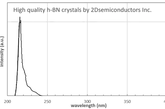
- 5.96 eV Bandgap — Deep-UV Optoelectronics: Solar-blind photodetectors and single-photon emitters operating at ~210-230 nm.
- 1,500°C Air Stability: Survives processing temperatures that destroy other 2D materials — CMOS BEOL compatible.
- HPHT & CVD Grades Available: HPHT bulk for highest-quality exfoliation; CVD films for wafer-scale device fabrication.
Research & References
hBN as Ultimate Dielectric for 2D Electronics — Review
Nature Reviews Materials, 2023 — Established hBN as the benchmark gate dielectric for 2D FETs, enabling graphene mobility >100,000 cm²/V·s — 10-100× higher than SiO2-gated devices. Practical takeaway: Princeton Powder's HPHT hBN crystals provide the pristine surface quality required for record-mobility 2D FET fabrication.
Wafer-Scale Single-Crystal hBN for Integrated 2D Electronics
Advanced Materials Interfaces, 2025 — Demonstrated CVD hBN on CuNi(111)/sapphire achieving single-crystal domains at wafer scale — the path to manufacturing-scale 2D devices. Practical takeaway: Princeton Powder's CVD hBN films on CuNi/sapphire enable the wafer-scale integration that 2D electronics requires for commercial viability.
Contact our 2D materials team for the full reference list.