
Tantalum Nitride (TaN) Sputtering Target — 4N Purity
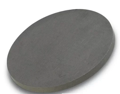
Princeton Powder is a leading supplier of high-purity (4N) Tantalum Nitride (TaN) sputtering targets, primarily used in thin-film deposition for the semiconductor and microelectronics industries. These targets are also suitable for applications in semiconductor manufacturing, chemical vapor deposition (CVD), physical vapor deposition (PVD), display technology, and optical and decorative coatings.
TaN targets are optimized for both direct current (DC) and radio frequency (RF) sputtering, depending on specific environmental needs. Impurity levels are tightly controlled. High flatness and an excellent surface finish are achieved. Optional backing materials, such as Copper or Molybdenum, are available. Tantalum Nitride sputtering targets are offered at competitive prices in the United States.
Material | Tantalum Nitride (TaN) sputtering targets |
CAS Number | 12033-62-4 |
Purity | 99.9%, 4N |
Shape | Discs, Plates, Column Targets, Step Targets, Custom-made |
| Density | 14.3 g/cm3 |
Melting Point | 3090 ℃ |
Dimensions | Dia.: 2.0″, 3.0″, 4.0″, 5.0″, 6.0″ Thick: 0.125″, 0.250″ |
Bonding | With Bonding, or customized |
Backing Material | Molybdenum Or Copper |
Product Overview
What is a TaN Sputtering Target?
A Tantalum Nitride (TaN) sputtering target is a high-purity (99.99% / 4N) ceramic-like compound target used in reactive DC/RF magnetron sputtering to deposit thin TaN films onto semiconductor wafers and other substrates. Princeton Powder supplies TaN sputtering targets in planar and rotary configurations with custom dimensions, bonded to copper or molybdenum backing plates for optimal thermal management during deposition.
Key Material Properties
| Composition | Tantalum Nitride (TaN) |
| Purity | 99.99% (4N) minimum |
| Density (thin film) | 13.7–14.3 g/cm³ (varies with N₂ flow ratio) |
| Resistivity | 200–400 μΩ·cm (tunable via N₂ partial pressure) |
| TCR | -50 to -100 ppm/°C (negative TCR — excellent for precision resistors) |
| Crystal Structure | Cubic (NaCl-type, fcc) for stoichiometric TaN; hexagonal for Ta₂N |
| Deposition Method | Reactive DC/RF magnetron sputtering from Ta target in Ar/N₂ atmosphere |
| Backing Plate | Oxygen-free Cu or Mo; bonded with indium or conductive elastomer |
Dimensions of Tantalum Nitride Sputtering Target
Circular Sputtering Targets | Diameter | 1.0” 2.0” 3.0” 4.0” 5.0” 6.0” Customized |
Rectangular Sputtering Targets | Width x Length | 5” x 12” 5” x 15” 5” x 20” 5” x 22” 6” x 20” Customized |
Thickness can be customized (With/No Bonding) | 0.125”, 0.25” Customized | |
Applications by Industry
Semiconductor Diffusion Barriers
TaN thin films are the industry-standard diffusion barrier between copper interconnects and silicon/dielectric layers in advanced semiconductor devices (45 nm node and below). TaN prevents Cu diffusion into the Si substrate — which would degrade transistor performance — while maintaining excellent adhesion to both Cu and low-k dielectrics. The film's amorphous/nanocrystalline structure provides superior barrier performance at thicknesses as low as 2-5 nm. Princeton Powder's 4N TaN targets ensure minimal trace metal contamination in these performance-critical applications.
Thin-Film Resistors (TFR)
Tantalum nitride is the material of choice for precision thin-film resistors in analog/mixed-signal ICs, RF modules, and high-reliability (space/military) electronics. TaN resistors offer excellent stability, low temperature coefficient of resistance (TCR ≈ -50 to -100 ppm/°C), and long-term reliability under thermal stress. The resistivity can be tuned by adjusting the N₂/Ar ratio during reactive sputtering, allowing a single target to serve multiple resistor values.
Optical & Decorative Coatings
TaN's gold-like appearance and exceptional corrosion resistance make it a popular decorative and protective coating for watches, jewelry, architectural hardware, and consumer electronics. Unlike actual gold plating, TaN coatings are extremely hard, scratch-resistant, and do not tarnish. In optical applications, TaN films serve as anti-reflection coatings and neutral-density filters where both optical performance and environmental durability are required.
Semiconductor Manufacturing: TaN serves as an effective diffusion barrier for copper interconnects, preventing copper migration into dielectric materials, which is critical for maintaining device integrity and performance.
Thin-Film Deposition: Used in the deposition of high-quality thin films in microelectronics, TaN contributes to improved performance in integrated circuits and electronic devices.
Chemical Vapor Deposition (CVD): TaN is utilized in CVD processes to create protective and functional coatings on various substrates, enhancing durability and performance.
Physical Vapor Deposition (PVD): In PVD applications, TaN targets are employed to produce hard, wear-resistant coatings, suitable for tools and components subjected to harsh conditions.
Optical Coatings: TaN films are used in optical applications due to their conductive properties, providing essential functionality in filters and mirrors.
Decorative Coatings: The aesthetic appeal and durability of TaN make it suitable for decorative coatings in consumer electronics and automotive applications.
Why Choose Princeton Powder for TaN Sputtering Targets
- 4N (99.99%) Certified Purity: Every TaN target includes GDMS (Glow Discharge Mass Spectrometry) trace element analysis — critical for semiconductor applications where ppb-level impurities affect device yield.
- Custom Dimensions & Configurations: Planar targets from 2" to 12" diameter; rotary targets for large-area coating. Custom thicknesses and backing plate configurations available.
- Bonding Services: In-house indium bonding and conductive elastomer bonding to Cu or Mo backing plates. Bond integrity verified via C-SAM (scanning acoustic microscopy).
- Target Reclamation: Spent target reclamation and re-bonding service — reduce your cost-per-wafer by reclaiming used backing plates with fresh TaN material.
- ISO 9001:2015 Certified: Quality management system ensures target-to-target consistency for production fabs where process repeatability is non-negotiable.
- US-Based Inventory & Fast Fulfillment: Stock targets ship within 5-10 business days; custom configurations quoted within 24 hours.
Ordering, Bonding & After-sales Support
Every TaN sputtering target order includes complete documentation: GDMS purity certificate, C-SAM bond integrity scan (if bonded), dimensional inspection report, and Certificate of Conformance. Standard lead time for stock targets is 5-10 business days; custom configurations require 3-5 weeks. All targets are packaged in vacuum-sealed, nitrogen-backfilled containers with shock-absorbent foam to prevent damage during transit. We ship globally with full export documentation. Contact our technical sales team at +1 (646) 749-1791 to discuss your target specifications or request a quote.
Frequently Asked Questions About TaN Sputtering Targets
What is the difference between TaN and TiN sputtering targets?
Both TaN and TiN serve as diffusion barriers in semiconductor manufacturing, but TaN offers superior barrier performance at thinner films (2-5 nm vs 5-10 nm for TiN) — critical for advanced nodes below 45 nm. TaN also has better adhesion to Cu and low-k dielectrics, and higher thermal stability. However, TiN is less expensive. Princeton Powder supplies both materials — contact our technical team for application-specific recommendations.
What purity grade do I need for semiconductor-grade TaN targets?
Semiconductor applications require 4N (99.99%) minimum purity. Princeton Powder's TaN targets are certified 4N with full GDMS trace element analysis provided. For non-semiconductor applications (decorative coatings, optical filters), 3N5 (99.95%) may be sufficient. Higher purity (4N5 / 99.995%) is available for R&D and advanced node development upon request.
How are TaN sputtering targets bonded to backing plates?
Princeton Powder offers two bonding methods: (1) Indium bonding — a low-temperature (156°C melting point) metallic bond providing excellent thermal and electrical conductivity, ideal for high-power DC sputtering; (2) Conductive elastomer bonding — a flexible polymer bond that accommodates thermal expansion mismatch, ideal for RF sputtering and lower power densities. Bond integrity is verified via C-SAM imaging with every order.
What is the typical target lifetime for a TaN sputtering target?
Target lifetime depends on power density, target thickness, and N₂/Ar ratio during reactive sputtering. A typical 6 mm thick TaN planar target operating at 5 W/cm² DC yields approximately 50-80 kW·h of useful life before re-bonding or replacement is needed. Princeton Powder provides expected lifetime estimates based on your specific process parameters — contact us with your deposition recipe for a calculation.
Can you reclaim and re-bond used TaN targets?
Yes. Princeton Powder offers a target reclamation service: we strip the spent TaN material from your backing plate, inspect the backing plate for damage/warpage, and bond fresh TaN material. This can reduce your per-target cost by 30-50% compared to purchasing new targets with backing plates each time. Contact us for a reclamation evaluation and quotation.
What documentation is provided with TaN target orders?
Every order includes: (1) GDMS purity certificate with full trace element analysis, (2) C-SAM bond integrity scan (for bonded targets), (3) Dimensional inspection report confirming diameter, thickness, and flatness against your specification, (4) Certificate of Conformance, (5) Commercial Invoice and Packing List for international shipments. Additional documentation (SEM micrographs, XRD phase analysis, resistivity test coupons) available upon request.
Research & Technical References
The following peer-reviewed research demonstrates TaN thin-film performance in key applications. Princeton Powder TaN sputtering targets meet or exceed the material specifications used in these studies.
TaN as a Cu Diffusion Barrier in Advanced Interconnects
Journal of Applied Physics, 2019 — Demonstrated that stoichiometric TaN films as thin as 3 nm provide effective Cu diffusion barrier performance at 450°C. Practical takeaway: For sub-10 nm node semiconductor manufacturing, TaN target purity and density uniformity are critical to achieving conformal 2-5 nm barrier films without pinholes.
Resistivity Tuning of TaN Thin Films via N₂ Partial Pressure
Thin Solid Films, 2020 — Showed that TaN film resistivity can be tuned from 200 to 2,000 μΩ·cm by varying N₂ flow rate during reactive sputtering, enabling a single target to produce both low-resistivity conductor films and high-resistivity resistor films. Practical takeaway: Princeton Powder's TaN targets support wide process windows for N₂/Ar ratio optimization — request a target optimized for your specific resistivity target.
Contact our technical team for the full reference list and to discuss how Princeton Powder TaN targets can meet your specific film requirements.