
Silicon Si Wafers: N & P Type, CZ & High-Resistivity FZ Wafers
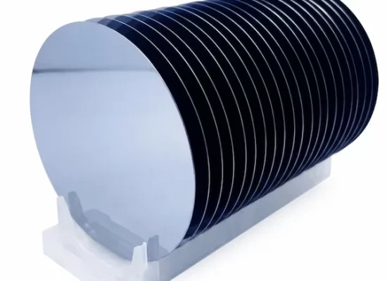
High-purity monocrystalline Silicon (Si) wafers serve as the foundational semiconductor substrate for integrated circuits, MEMS fabrication, sensors, and photovoltaic devices. Available in N-type (Phosphorus/Arsenic/Antimony doped) and P-type (Boron doped) configurations, these substrates are engineered for precise electrical resistivity. Choose between economical Czochralski (CZ) growth for general microelectronics or ultra-pure Float Zone (FZ) growth for high-resistivity RF and power device applications.
We supply Si wafers across standard (100), (111), and (110) crystallographic orientations in single-side (SSP) or double-side polished (DSP) finishes. Available in 2″ to 12″ diameters with custom thermal oxidation, thickness, and prime/test grading. Contact us for bulk OEM orders.
Technical Specifications
| Product | Si — Single Crystal Silicon Wafer, Diamond Cubic, Fd3m |
| Bandgap / Density | 1.12 eV (indirect) | 2.33 g/cm³ |
| Melting Point / Hardness | 1,414°C | Mohs 7 |
| Doping Types | N-type (P: 0.001->20k Ω·cm; As: 0.001-0.008; Sb) | P-type (B: 0.001->1k Ω·cm) | Intrinsic FZ: >1k->20k Ω·cm |
| Growth Methods | CZ (Czochralski — 1-300 Ω·cm, general semiconductor) | FZ (Float Zone — >1k Ω·cm, RF/power, ultra-pure) |
| Wafer Diameters | 1″–12″ (25-300mm) — full semiconductor industry range |
| Orientations | <100> (CMOS), <111> (bipolar/power), <110> ±0.5° |
| Polish / Ra | SSP/DSP/P/E; CMP Ra<0.5nm; optional SiO2 (100nm-2µm), Pt-coated, Si3N4 |
| Primary Applications | IC/MEMS/power/RF device fabrication, R&D substrates, process monitoring, mechanical fixturing |
Product Overview
Silicon wafers are the foundation of the global semiconductor industry — the substrate on which >90% of all ICs, power devices, MEMS sensors, and photonic components are fabricated. Princeton Powder supplies N-type (Phosphorus, Arsenic, Antimony) and P-type (Boron) wafers in both CZ and FZ growth, <100><111><110>, 1″-12″, resistivity 0.001->20,000 Ω·cm, Prime/Test/Dummy grades, CMP polished (SSP/DSP Ra<0.5nm), with optional thermal SiO2 and Pt metallization.
Technical Specifications
| Parameter | Specification |
|---|---|
| Crystal Structure | Diamond cubic, Fd3m, a=5.431Å |
| Bandgap / Density / Melting | 1.12 eV | 2.33 g/cm³ | 1,414°C |
| N-type Dopants | P: 0.001->20k Ω·cm; As: 0.001-0.008 Ω·cm; Sb available |
| P-type Dopant / Intrinsic | B: 0.001->1k Ω·cm | FZ Intrinsic: >1k->20k Ω·cm (undoped) |
| Growth: CZ / FZ | CZ: 1-300 Ω·cm (general semiconductor) | FZ: >1k Ω·cm (RF/power, ultra-pure) |
| Diameters | 1″-12″ (25-300mm); thickness 200-1,000µm ±10-25µm |
| Orientations | <100> (CMOS), <111> (bipolar/power), <110> ±0.5° |
| Polish / Ra | SSP/DSP/P/E; CMP Ra<0.5nm |
| TTV/Bow/Warp | ≤10-15µm / ≤40-65µm / ≤40-65µm (grade & diameter dependent) |
| Grades | Prime (device-quality) | Test (monitoring) | Dummy (mechanical) | Mechanical |
| Options | Thermal SiO2 (100nm-2µm), Pt-coated, LPCVD Si3N4, SOI wafers |
Characteristics
| Product metric | Units | Prime Standard | Test Grade |
|---|---|---|---|
| Crystal Characteristics | |||
| Polytype | 4H | 4H | |
| Doping Type | n-type | n-type | |
| Dopant | Nitrogen | Nitrogen | |
| Surface Orientation | degrees | 3.8 – 4.2 | – |
| Wafer Mechanical Characteristics | |||
| Diameter | mm | 99.7 – 100 | 99.5 – 100 |
| Thickness | μm | 330 – 370 | 325 – 375 |
| Primary Flat Position | degree | ± 1 | ± 1 |
| Primary Flat Length | mm | 31.5 – 34 | 30.5 – 34.5 |
| Secondary Flat Position | mm | ± 5 | ± 5 |
| Secondary Flat Length | mm | 17.5 – 19.5 | 16 – 20 |
| Bow | μm | ± 20 | R |
| Warp | μm | ≤ 30 | R |
| Total Thickness Variation (TTV) | μm | ≤ 5 | R |
| Local Thickness Variation (SBIR) | μm | ≤ 2 | R |
| Substrate Quality | |||
| Resistivity | ohm-cm | 0.014 – 0.024 | 0.010 – 0.030 |
| Foreign Polytypes | % | 0 | ≤ 15 |
| Defects (TUA)1 | % | ≥ 95 | nr |
| Dislocation Distribution2 (EPD) | cm-2 | ≤ 12,000 | nr |
| TED | cm-2 | ≤ 9,000 | nr |
| TSD | cm-2 | ≤ 1,000 | nr |
| BPD | cm-2 | ≤ 2,000 | nr |
| MPD | cm-2 | ≤ 0.5 | nr |
| Surface and crystal imperfections | cm-2 | ≤ 1 | na |
| Hex Plates | % | 0 | nr |
| Visual Carbon Inclusion | % area | < 0.05 | nr |
| Visual Edge Inclusions | number | 0 | nr |
| Visible Scratches | mm | < 15 | nr |
| Edge Chips and Indents | number | 0 | Yes; not quantified |
| Cracks | number | 0 | 0 |
| Pinholes | number | 0 | Yes; not quantified |
| Pits | number | < 5 | nr |
| Surface Quality | |||
| Silicon face finish3 | nm | < 0.5 | Mirror |
| Carbon face finish3 | nm | ≤ 5 | Mirror |
| Metal Contamination4 (Al, Cr, Fe, Ni, Cu, Zn, Hg, Na*, K, Ti, Ca & Mg) | atoms/cm2 | ≤ 1e+11 (except LDL for Al & Na as noted) | R |
| Contamination | % | None | R |
| Particle Contamination | number | ||