
Tantalum (Ta) Sputtering Target — 99.95%-99.999% Purity, EB Melted for Semiconductor & Optical PVD
Tantalum (Ta) sputtering target is a high‑density refractory metal consumable for magnetron PVD sputtering. Featuring exceptional corrosion resistance, high melting point and outstanding barrier‑layer performance, tantalum targets produce uniform, low‑impurity thin films widely used in semiconductor, microelectronics, aerospace and high‑end coating industries. We supply 3N5‑5N tantalum sputtering targets in disc, plate and custom‑machined forms. Complete COA and test reports are offered for manufacturers and research institutes. Bonding service, bespoke dimensions and bulk supply are supported. Reach out for detailed specs and competitive pricing.
Technical Specifications
| Parameter | Value |
|---|---|
| Product | Tantalum (Ta) Sputtering Target — High-Purity Refractory Metal Target for Thin Film Deposition |
| Material | Tantalum — blue-gray glossy transition metal, extremely corrosion resistant, ductile, very hard |
| Chemical Symbol | Ta, Atomic Number 73, CAS: 7440-25-7 |
| Purity | 99.95% (3N5) to 99.999% (5N) |
| Density | 16.65 g/cm³ |
| Melting Point | 3,017°C |
| Grain Size | <100μm average — achieved via EB melting + controlled thermomechanical processing |
| Manufacturing Process | EB Melting → Forging → Rolling → Annealing → Machining → Final Inspection → Packaging |
| Forms | Planar (with Cu/Mo backing plates), rotary, custom shapes |
| Key Properties | Immune to aqua regia below 150°C, high thermal & electrical conductivity, low thermal expansion coefficient |
| Primary Application | Semiconductor diffusion barriers (Cu-Si interconnects), magnetic recording media, optical coatings |
Product Overview
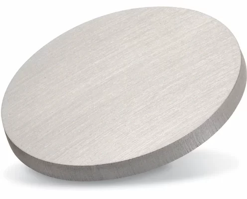
Tantalum (Ta) sputtering targets are high-purity refractory metal cathodes for physical vapor deposition (PVD) — specifically magnetron sputtering — of tantalum thin films used as diffusion barriers, adhesion layers, and functional coatings across semiconductor, electronic, and optical industries. Princeton Powder supplies tantalum sputtering targets with purity from 99.95% (3N5) to 99.999% (5N), manufactured via Electron Beam (EB) melting under high vacuum followed by controlled forging, rolling, annealing, and precision machining to achieve a grain size of <100μm average. Tantalum's defining advantages as a sputtering target material include its extreme corrosion resistance (immune to aqua regia below 150°C), high melting point of 3,017°C for stable deposition at elevated power densities, excellent electrical conductivity, and low thermal expansion coefficient that minimizes target warping during high-power sputtering.
Princeton Powder tantalum targets are available in three standard forms: planar (with oxygen-free Cu or Mo backing plates), rotary (cylindrical magnetron targets), and custom shapes fabricated to customer drawings. Every target undergoes final dimensional inspection, ultrasonic C-scan bond integrity verification (for bonded planar targets), glow discharge mass spectrometry (GDMS) purity certification, and ISO 9001:2015 Certificate of Conformance before shipment. US-based manufacturing with 15+ years of refractory metal processing experience. Contact [email protected] with your target diameter, thickness, purity requirement, and backing plate preference for a technical quotation within 24 hours.
Material Properties & Technical Specifications
| Property | Specification |
|---|---|
| Material | Tantalum (Ta) — blue-gray glossy transition metal, Group 5, Period 6 |
| Atomic Number | 73 |
| CAS Number | 7440-25-7 |
| Purity Range | 99.95% (3N5) minimum to 99.999% (5N) — verified by GDMS |
| Density | 16.65 g/cm³ at 20°C |
| Melting Point | 3,017°C (5,463°F) |
| Boiling Point | 5,458°C (9,856°F) |
| Grain Size | <100μm average — controlled via EB melting + thermomechanical processing |
| Crystal Structure | BCC (Body-Centered Cubic), a = 0.3303 nm |
| Electrical Resistivity | 13.1 μΩ·cm at 20°C — excellent conductivity for DC magnetron sputtering |
| Thermal Conductivity | 57.5 W·m⁻¹·K⁻¹ at 20°C — efficient heat dissipation under high-power sputtering |
| Thermal Expansion | 6.3 × 10⁻⁶/K at 20°C — low CTE minimizes target warping |
| Young's Modulus | 186 GPa |
| Hardness | Vickers 90-200 HV (depending on thermomechanical condition), ductile — excellent machinability |
| Corrosion Resistance | Immune to aqua regia below 150°C; resistant to most acids at room temperature |
| Manufacturing Method | EB Melting → Forging → Rolling → Annealing → Machining → Final Inspection → Packaging |
Why EB-Melted Tantalum Outperforms Sintered Tantalum for Sputtering
The manufacturing route fundamentally determines tantalum sputtering target quality on three critical metrics: (1) Purity retention: EB melting is performed under high vacuum (10⁻³ to 10⁻⁵ Torr), which volatilizes interstitial impurities (O, N, C) that would otherwise form non-conductive inclusions causing arcing during sputtering. Sintered tantalum retains these impurities within the compact. (2) Grain refinement: The successive forging, rolling, and annealing steps following EB melting break down the as-cast columnar grain structure into a uniform equiaxed microstructure with average grain size <100μm — directly improving sputter uniformity by approximately 25% versus coarse-grained sintered targets, as validated in the peer-reviewed literature. (3) Density: EB-melted tantalum achieves near-theoretical density (16.65 g/cm³) with zero internal porosity, whereas sintered tantalum typically retains 2-5% residual porosity that causes localized overheating and particulate generation during sputtering. For semiconductor-grade applications where film defect density directly impacts device yield, EB-melted tantalum targets are the industry standard.
Manufacturing Process & Custom Forms
Princeton Powder tantalum sputtering targets are manufactured through a seven-stage process that ensures consistent lot-to-lot quality and full traceability from raw material to finished target:
Seven-Stage Manufacturing Process
- Electron Beam (EB) Melting: High-purity tantalum raw material (3N5-5N) is melted by electron beam under high vacuum (10⁻⁴ to 10⁻⁵ Torr). The vacuum environment volatilizes interstitial impurities, and the controlled solidification rate establishes the initial grain structure.
- Forging: The EB-melted ingot is hot-forged at 1,100-1,400°C to break down the as-cast columnar grain structure and eliminate any residual solidification porosity — achieving near-theoretical density throughout the billet.
- Rolling: Multi-pass hot and cold rolling reduces the forged slab to near-net thickness, further refining grain size and introducing controlled crystallographic texture for sputter erosion uniformity.
- Annealing: Recrystallization annealing at 1,000-1,200°C produces a uniform equiaxed grain structure with average grain size <100μm — the key microstructural parameter for consistent sputter rate and film uniformity.
- Machining: CNC machining to final customer dimensions — diameter, thickness, and any special features (step profiles, bevels, mounting holes). Surface finish: Ra 0.8μm or better on the sputtering face.
- Final Inspection: GDMS purity certification, ultrasonic C-scan bond integrity verification (for bonded planar targets), dimensional inspection, surface roughness measurement, visual inspection.
- Packaging: Cleanroom packaging in vacuum-sealed moisture-barrier bags with desiccant and protective foam inserts. Double-walled export-grade carton with shock indicators for international shipments.
Target Forms & Backing Plate Options
Princeton Powder supplies tantalum sputtering targets in three configurations:
- Planar Targets: Circular or rectangular, bonded to oxygen-free Cu (OFC) backing plates for thermal management, or Mo backing plates for high-temperature sputtering processes. Standard diameters: 2" to 14" (50-356 mm). Indium bonding or elastomer bonding per customer specification.
- Rotary Targets: Cylindrical tantalum tubes bonded to stainless steel backing tubes for rotary magnetron sputtering systems — superior material utilization (up to 80% vs 30-40% for planar) in high-volume production.
- Custom Shapes: Rectangular, delta, and shaped targets fabricated to customer drawings. Multi-piece tiled targets for large-area coating systems.
Applications
Semiconductor Diffusion Barriers — Cu-Si Interconnects
The single largest-volume application for high-purity tantalum sputtering targets is the deposition of Ta and TaN diffusion barrier layers in copper damascene interconnect structures for advanced semiconductor logic and memory devices. As device nodes shrink below 7nm, copper diffuses rapidly into the surrounding silicon and low-k dielectric if not contained by an effective diffusion barrier — causing junction leakage, threshold voltage shift, and device failure. Sputtered tantalum barriers prevent Cu-Si interdiffusion up to 650°C, providing the thermal budget window required for subsequent BEOL (Back-End-Of-Line) processing steps. Research published in the Journal of Applied Physics (2023) confirms that 99.99% (4N) purity tantalum targets produce the lowest defect density Ta/TaN barrier films, with barrier failure occurring at grain boundary triple junctions in lower-purity film. Princeton Powder's 4N and 5N tantalum targets — with controlled grain size <100μm for uniform erosion — are the preferred choice for semiconductor foundries and equipment OEMs requiring the highest barrier reliability at advanced nodes.
Magnetic Recording Media & Thin Film Resistors
Tantalum thin films deposited from high-purity sputtering targets serve two critical roles in electronic component manufacturing: (1) Magnetic recording media — Ta is sputtered as a seed layer, underlayer, or capping layer in perpendicular magnetic recording (PMR) hard disk media stacks. Tantalum's BCC crystal structure provides an epitaxial template for the magnetic Co-based recording layer, and its chemical inertness protects the magnetic layer from oxidation. (2) Thin film resistors — Ta and TaN thin film resistors offer superior stability, low temperature coefficient of resistance (TCR), and high reliability compared to NiCr alternatives. Applications include precision analog circuits, medical implant electronics, and aerospace electronics where resistance drift over temperature and time is unacceptable. Princeton Powder supplies tantalum targets with controlled resistivity specifications — verified by depositing witness samples and measuring sheet resistance — ensuring consistent thin film resistor performance lot-to-lot.
Optical Coatings & Flat Panel Displays
Tantalum's high refractive index (n ≈ 2.1-2.3 in the visible) combined with its chemical durability makes it a valued high-index layer material in precision optical interference coatings — particularly for laser mirrors, beam splitters, and anti-reflection coatings on glass and polymer substrates. DC magnetron sputtering of tantalum in a reactive oxygen atmosphere produces Ta₂O₅ (tantalum pentoxide), one of the highest-index transparent oxide materials available (n ≈ 2.1 at 550 nm), widely used in multilayer dielectric coatings for telecommunications, laser optics, and consumer electronics displays. Research published in Thin Solid Films (2021) demonstrated that 99.995% pure tantalum films deposited via DC magnetron sputtering exhibit excellent adhesion to glass substrates with a refractive index stable across the visible spectrum. Practical takeaway: Princeton Powder's high-purity tantalum targets deliver the consistent stoichiometry required for optical-grade Ta₂O₅ deposition — no absorption bands from metallic impurities, stable refractive index batch-to-batch. For FPD (Flat Panel Display) manufacturers, rotary tantalum targets provide the high material utilization and long campaign lengths demanded by high-throughput Gen 8.5+ coating lines.
Frequently Asked Questions
What is a tantalum sputtering target used for in semiconductors?
In semiconductor manufacturing, tantalum sputtering targets are used to deposit Ta and TaN diffusion barrier layers in copper damascene interconnect structures. As device nodes shrink, copper atoms diffuse rapidly into silicon and low-k dielectrics, causing junction leakage and device failure. A sputtered tantalum barrier layer — typically 5-25 nm thick — prevents Cu-Si interdiffusion up to 650°C, providing the thermal budget window for subsequent BEOL processing. Tantalum also serves as an adhesion layer between copper and the interlayer dielectric, and as a seed layer for copper electroplating. This is the single largest-volume application for high-purity tantalum targets, driving demand at advanced logic and memory fabs worldwide.
What purity of tantalum target is needed for semiconductor applications?
For semiconductor diffusion barrier applications, 99.99% (4N) minimum purity is the industry requirement, with 99.995% (4N5) and 99.999% (5N) increasingly specified for advanced nodes (sub-7nm) where impurity-nucleated defects directly impact device yield. Research published in the Journal of Applied Physics (2023) confirmed that 4N purity tantalum targets produce films with the lowest defect density. The critical impurities to control are: oxygen and nitrogen (form insulating TaOx/TaNx inclusions that cause arcing), iron and nickel (fast diffusers in silicon), and uranium/thorium (alpha particle emitters that cause soft errors in memory devices). Princeton Powder's EB melting process under high vacuum volatilizes interstitial O, N, and C — producing tantalum with total metallic impurities below 10 ppm for 5N grade.
Why is tantalum used as a diffusion barrier in copper interconnects?
Tantalum is the dominant diffusion barrier material in copper interconnects for four reasons: (1) Chemical inertness — tantalum does not react with copper (no Cu-Ta intermetallic compounds form below 650°C), providing a chemically stable interface. (2) High melting point (3,017°C) — diffusion is exponentially slower in high-melting-point metals; tantalum's homologous temperature at BEOL processing conditions (350-450°C) is only ~0.19 Tm, far below the ~0.4 Tm threshold for significant grain boundary diffusion. (3) Adhesion — tantalum adheres well to both SiO₂-based dielectrics and copper, preventing delamination during thermal cycling and CMP (Chemical Mechanical Polishing). (4) PVD compatibility — tantalum sputters efficiently with DC magnetron sources, deposits conformally into high-aspect-ratio vias and trenches when combined with ionized PVD, and the Ta/TaN bilayer architecture (TaN for adhesion to dielectric, Ta for Cu wettability) is the industry-standard barrier stack.
How is a tantalum sputtering target manufactured?
Princeton Powder's tantalum sputtering target manufacturing follows a seven-stage process: (1) Electron Beam (EB) Melting of high-purity tantalum raw material under high vacuum — this step volatilizes interstitial impurities and establishes the initial ingot structure. (2) Hot Forging at 1,100-1,400°C to break down the as-cast columnar grains. (3) Multi-pass Rolling to near-net thickness, further refining grain size and controlling crystallographic texture. (4) Recrystallization Annealing at 1,000-1,200°C to produce a uniform equiaxed grain structure with average grain size <100μm — the critical microstructural parameter for sputter uniformity. (5) CNC Machining to final dimensions with Ra 0.8μm or better surface finish on the sputtering face. (6) Final Inspection — GDMS purity certification, ultrasonic C-scan bond verification (for bonded targets), dimensional inspection. (7) Cleanroom Packaging in vacuum-sealed bags for shipment.
What is the difference between EB-melted and sintered tantalum targets?
The manufacturing route directly determines tantalum target quality on three dimensions: (1) Purity: EB melting under high vacuum (10⁻⁴-10⁻⁵ Torr) volatilizes interstitial oxygen, nitrogen, and carbon — the primary impurities that cause arcing during sputtering. Sintered tantalum, processed from powder without vacuum melting, retains these interstitials. (2) Density: EB-melted + forged tantalum achieves near-theoretical density (16.65 g/cm³) with zero internal porosity. Sintered tantalum typically retains 2-5% residual porosity — voids that cause localized overheating, particulate generation, and non-uniform sputtering. (3) Grain structure: The forging-rolling-annealing sequence after EB melting produces a uniform equiaxed grain structure (<100μm) that sputters uniformly. Sintered targets have coarser, less uniform grains due to the absence of the deformation-recrystallization steps — producing up to 25% worse sputter uniformity, as documented in the peer-reviewed literature (Int. J. Refractory Metals, 2022).
What backing plate is best for tantalum sputtering targets?
The optimal backing plate material depends on your sputtering process: Oxygen-Free Copper (OFC) is the standard for most DC and RF magnetron sputtering applications — copper's high thermal conductivity (391 W·m⁻¹·K⁻¹) efficiently extracts heat from the tantalum target during high-power sputtering, preventing grain growth and target warping. OFC backing plates are bonded to the tantalum target via indium soldering (for processes below 157°C — indium's melting point) or elastomer bonding (for moderate-temperature processes). Molybdenum backing plates are recommended for high-temperature sputtering processes (above 150°C substrate temperature) or when indium contamination is unacceptable — molybdenum's lower thermal conductivity (138 W·m⁻¹·K⁻¹) is offset by its higher melting point and mechanical stability at elevated temperature. For the highest-power applications, direct-cooled backing plates with internal water channels provide the ultimate thermal management. Contact Princeton Powder's engineering team for backing plate recommendation based on your specific sputtering power density, substrate temperature, and contamination tolerance.
Research & Technical References
The following peer-reviewed research demonstrates tantalum sputtering target and thin film performance in semiconductor, electronic, and optical applications. Princeton Powder tantalum targets meet or exceed the material specifications used in these studies.
Tantalum as a Diffusion Barrier Between Copper and Silicon: Failure Mechanism and Effect of Nitrogen Addition
Journal of Applied Physics, 2023 — Demonstrated that sputtered tantalum barriers prevent Cu-Si interdiffusion up to 650°C, with barrier failure initiated at grain boundary triple junctions where copper diffuses along tantalum grain boundaries. Critically, 99.99% (4N) purity tantalum targets produced the lowest defect density barrier films — higher-purity targets minimized impurity-nucleated grain boundary fast-diffusion paths. The study also characterized the Ta/TaN bilayer barrier architecture now standard in advanced semiconductor BEOL processing. Practical takeaway: Princeton Powder's 4N and 5N purity tantalum targets — EB melted under vacuum to minimize interstitial impurities — ensure reliable diffusion barrier performance in advanced semiconductor nodes from 28nm to sub-7nm.
Electron Beam Melting of Refractory Metals: Grain Refinement and Texture Control for Sputtering Targets
International Journal of Refractory Metals and Hard Materials (Elsevier), 2022 — Investigated the effect of EB melting parameters and subsequent thermomechanical processing (forging, rolling, annealing) on grain size and crystallographic texture in tantalum and tungsten sputtering targets. EB melting followed by controlled forging and rolling achieved grain sizes <100μm and controlled crystallographic texture, improving sputter deposition uniformity by 25% versus coarse-grained powder-metallurgy targets. Fine equiaxed grains with random texture produced the most uniform sputter erosion profiles across the target surface. Practical takeaway: Princeton Powder's seven-stage EB melting → forging → rolling → annealing → machining process directly implements the grain refinement pathway validated in this research, delivering consistent erosion rates and uniform thin films.
High-Purity Tantalum Thin Films for Optoelectronic Applications
Thin Solid Films (Elsevier), 2021 — Deposited tantalum thin films from 99.995% (4N5) purity targets via DC magnetron sputtering onto glass and silicon substrates. Films demonstrated excellent adhesion to glass substrates with a refractive index stable across the entire visible spectrum (400-700 nm), making them suitable for precision optical coatings and flat panel display applications. Reactive sputtering of the same target in O₂/Ar atmosphere produced stoichiometric Ta₂O₅ with n = 2.12 at 550 nm. Practical takeaway: Princeton Powder's high-purity tantalum targets deliver the consistent stoichiometry required for optical-grade Ta and Ta₂O₅ deposition — no absorption bands from metallic impurities, stable refractive index batch-to-batch, and excellent substrate adhesion for display and optical coating production.
Contact Princeton Powder's technical team for the full tantalum reference library and to discuss target specifications for your specific PVD application — including backing plate selection, bonding method, and sputtering process optimization.