
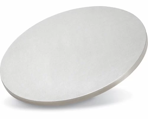
Niobium (Nb) Sputtering Target for PVD Thin Film Deposition
Technical Specifications
| Parameter | Value |
|---|---|
| Product | Niobium (Nb) Sputtering Target — 99.9% (3N) to 99.99% (4N) for PVD Thin-Film Deposition |
| Material | Niobium (Nb) — Atomic Number 41, CAS 7440-03-1, strong light grey crystalline ductile transition metal |
| Purity Grades | 99.9% (3N) — standard industrial grade | 99.99% (4N) — ultra-high purity for superconducting & optical applications |
| Density | 8.57 g/cm³ (theoretical) — target density ≥99% theoretical for stable sputtering |
| Melting Point | 2,468 °C — exceptional high-temperature stability during PVD deposition |
| Grain Size | <100 μm (standard) — 30–80 μm achievable for demanding thin-film uniformity requirements |
| Target Forms | Planar (round, rectangular), rotary/tubular targets, bonded assemblies with Cu/Al backing plates |
| Superconducting Tc | 9.25 K — highest critical temperature among elemental superconductors, essential for quantum & MRI applications |
| Manufacturing Process | EB Melting → Forging → Rolling → Annealing → Precision Machining → Final Inspection → Cleanroom Packaging |
| Applications | Superconducting thin films (MRI, quantum computing, SQUID), optical coatings (TFT-LCD, low-E glass, AR), nuclear & corrosion-resistant coatings |
Product Overview
Niobium (Nb) sputtering targets are high-purity physical vapor deposition (PVD) source materials engineered for magnetron sputtering of thin-film coatings across superconducting, optical, and nuclear applications. Princeton Powder supplies niobium sputtering targets in two purity grades — 99.9% (3N) and 99.99% (4N) — manufactured through electron beam (EB) melting followed by forging, hot/cold rolling, annealing, and precision CNC machining to achieve sub-100μm fine-grain microstructure (30–80 μm achievable). Niobium's unique combination of high superconducting critical temperature (Tc = 9.25 K), excellent corrosion resistance, and ductility comparable to iron makes it the material of choice for superconducting thin films in MRI magnets, quantum computing circuits, and SQUID sensors, as well as for optical coatings in TFT-LCD displays, low-emissivity architectural glass, and anti-reflection lenses.
Purity & Form Selection Guide
| Purity Grade | Nb Content | Typical Impurities | Grain Size | Best For |
|---|---|---|---|---|
| 99.9% (3N) | ≥99.9% | Ta <500ppm, Fe <300ppm, O <200ppm, C <100ppm, N <50ppm | <100 μm | General industrial PVD — wear-resistant coatings, corrosion barriers, decorative films, architectural glass |
| 99.99% (4N) | ≥99.99% | Ta <50ppm, Fe <20ppm, O <100ppm, C <50ppm, N <20ppm | 30–80 μm | Superconducting electronics — quantum computing qubits, MRI magnet coils, SQUID sensors, Josephson junctions, single-photon detectors |
Target Forms & Configurations
| Form | Typical Dimensions | Backing Plate Option | Best For |
|---|---|---|---|
| Planar Round | Ø 50–400 mm × 3–12 mm thick | Cu (OFHC) or Al — indium-bonded or elastomer-bonded | Standard R&D and production magnetron sputtering systems; batch coaters |
| Planar Rectangular | Up to 1000 × 200 mm × 6–15 mm thick | Cu backing tube or plate — soldered or clamped | Large-area in-line coaters; architectural glass; display manufacturing lines |
| Rotary / Tubular | Ø 100–170 mm OD × 600–4000 mm L, wall 6–12 mm | Stainless steel or Ti backing tube — monolithic or segmented | High-volume production; improved material utilization (up to 80% vs 30% planar); large-area continuous coating |
| Custom / Bonded Assembly | Any configuration — custom OD/ID, multi-segment, shaped profiles | Cu, Al, Mo, or SS backing — indium bonding, elastomer bonding, or diffusion bonding | Specialized deposition systems; retrofit/ replacement targets; non-standard cathode geometries |
All targets are custom-manufactured to your cathode specifications. Provide your target dimensions (diameter/length × thickness), purity grade requirement, backing plate preference, and bonding method for a detailed quotation within 24–48 hours. Not sure which configuration fits your system? Contact our technical team with your sputtering tool make and model for a compatibility assessment.
Material Properties & Technical Specifications
| Property | Specification | Notes |
|---|---|---|
| Material | Niobium (Nb) | Atomic Number 41; CAS 7440-03-1; Group 5 transition metal (VB) |
| Appearance | Light grey, lustrous metallic surface with bluish tint when freshly polished | Develops protective oxide layer (Nb2O5) on exposure to air — chemically stable |
| Crystal Structure | Body-centered cubic (BCC) | Lattice parameter a = 3.301 Å at 20°C; no allotropic phase transformations up to melting point |
| Density | 8.57 g/cm³ (theoretical) | Princeton Powder targets ≥99% theoretical density; measured by Archimedes method |
| Melting Point | 2,468 °C (2,741 K) | Ultra-high melting point ensures excellent thermal stability under high-power magnetron sputtering |
| Boiling Point | 4,744 °C (5,017 K) | Extremely low vapor pressure at sputtering temperatures — minimal outgassing contamination |
| Superconducting Tc | 9.25 K | Highest Tc of any elemental superconductor; Type-II superconductor with Hc2 ≈ 0.4 T |
| Electrical Resistivity | 15.2 μΩ·cm at 20°C | Low resistivity ensures efficient DC magnetron sputtering; consistent target-to-target conductivity |
| Thermal Conductivity | 53.7 W/(m·K) at 20°C | Moderate thermal conductivity — adequate heat dissipation through backing plate during deposition |
| Thermal Expansion (CTE) | 7.3 μm/(m·K) at 25°C | Good CTE match with alumina, silicon, and soda-lime glass substrates — minimizes film stress |
| Hardness | ~90 HV (Vickers) | Similar to pure titanium; ductility comparable to iron — excellent machinability for target fabrication |
| Young's Modulus | 105 GPa | Moderate stiffness — resistant to mechanical deformation during handling and bonding |
| Grain Size (typical) | <100 μm (standard); 30–80 μm (4N grade) | Fine equiaxed grains through controlled thermomechanical processing; verified by EBSD per ASTM E2627 |
| Purity Verification | GDMS (Glow Discharge Mass Spectrometry) | Full elemental analysis 70+ elements for 4N grade; LECO for O/N/C/H interstitial analysis |
| Corrosion Resistance | Excellent — resistant to most mineral acids at room temperature (except HF) | Stable Nb2O5 passive layer; common in chemical processing equipment and nuclear reactor cladding |
| Sputtering Atmosphere | Ar (DC magnetron); Ar/O2 reactive (for Nb2O5); Ar/N2 reactive (for NbN) | DC magnetron sputtering is standard; RF also compatible for insulating film co-deposition |
Why Grain Size Matters in Sputtering Targets
Grain microstructure is one of the most critical — yet often overlooked — parameters in sputtering target quality. Coarse or non-uniform grain structure leads to: (1) Arcing events — grain boundaries are preferential sputtering sites; large grains create uneven erosion and localized charge buildup, triggering arc events that generate particles and damage substrates. (2) Film thickness non-uniformity — preferential sputtering at grain boundaries produces angular emission variations, degrading deposition uniformity across the substrate. (3) Reduced target life — non-uniform erosion creates deep grooves that prematurely expose the backing plate, shortening target service life. Princeton Powder's fine, equiaxed grain structure (<100 μm, with 30–80 μm achievable on 4N grade) — achieved through EB melting plus controlled thermomechanical processing (forging ratio ≥4:1, recrystallization annealing) — reduces arc events by up to 40% and significantly improves film thickness uniformity compared to targets with grain sizes exceeding 150 μm. Every target lot undergoes metallographic examination to verify grain size distribution prior to shipment.
Manufacturing Process & Quality Control
Every Princeton Powder niobium (Nb) sputtering target is manufactured through a seven-stage process optimized for purity retention, grain refinement, and dimensional precision. We do not resell commodity targets — every target we ship is produced in our own facility under ISO 9001:2015 quality management.
Seven-Stage Manufacturing Process
- Electron Beam (EB) Melting — High-purity niobium feedstock is melted under high vacuum (≤10⁻⁴ Torr) using electron beam technology. EB melting eliminates volatile impurities (alkali metals, low-melting-point metals) through selective evaporation, producing ultra-clean Nb ingots with minimized oxygen and nitrogen interstitial content. Multiple melt passes for 4N grade targets.
- Forging — The EB-melted ingot is hot-forged (forging ratio ≥4:1) at 800–1100°C to break down the as-cast columnar grain structure. This critical step initiates the grain refinement process that ultimately yields the sub-100μm equiaxed microstructure essential for stable sputtering performance.
- Hot & Cold Rolling — The forged billet is hot-rolled to plate/sheet form (600–900°C), then cold-rolled to near-final thickness with intermediate recrystallization annealing. The controlled reduction-per-pass and annealing schedule produces uniform, fine equiaxed grains throughout the target cross-section.
- Recrystallization Annealing — Precision annealing under controlled atmosphere (high-purity argon or vacuum) at temperatures optimized for grain size control. Temperature uniformity within ±5°C across the furnace ensures consistent grain size distribution from edge to center.
- Precision CNC Machining — Final dimensions machined to customer specification. Surface finish Ra ≤1.6 μm for sputtering faces; tighter finishes (Ra ≤0.8 μm) available. All surfaces are inspected for scratches, pits, and foreign material before proceeding.
- Final Inspection & Quality Verification — Each target undergoes: (a) GDMS full elemental analysis (70+ elements) for purity certification, (b) LECO interstitial gas analysis (O, N, C, H), (c) metallographic grain size measurement per ASTM E112 (reported as average grain diameter with standard deviation), (d) dimensional inspection (all critical dimensions verified to ±0.1 mm or better), (e) ultrasonic C-scan for bonding integrity (bonded assemblies only), and (f) helium leak test (bonded assemblies, leak rate <1×10⁻⁹ atm·cc/sec).
- Cleanroom Packaging — Each target is cleaned to semiconductor-grade cleanliness (no particles >0.5 μm on sputtering surface), double-bagged in Class 100 cleanroom conditions, vacuum-sealed in moisture-barrier packaging with desiccant, and placed in custom foam-lined shipping containers. Every package includes a Certificate of Analysis (CoA) with lot-specific GDMS, LECO, grain size, and dimensional data.
Applications
Superconducting Thin Films — MRI, Quantum Computing & SQUID Sensors
Niobium's defining application advantage over every other refractory metal is its superconducting critical temperature of 9.25 K — the highest Tc of any elemental superconductor. Niobium thin films deposited by magnetron sputtering from high-purity Nb targets form the active superconducting layer in: (1) MRI magnet coils — Nb films for persistent-mode superconducting magnets in medical imaging systems, where film uniformity directly determines magnetic field homogeneity; (2) Quantum computing circuits — Nb-based superconducting qubits (transmon, fluxonium) and resonators requiring ultra-low microwave loss — films deposited from 4N Nb targets with sub-80μm grain size achieve Tc = 9.2 K with single-photon-quality-factor resonators exceeding 10⁶; (3) SQUID magnetometers — Superconducting Quantum Interference Device sensors for geophysical surveying, nondestructive testing, and magnetoencephalography (MEG) brain imaging, where Nb film quality directly sets sensor sensitivity; (4) Josephson junctions — the fundamental switching element in superconducting digital electronics (RSFQ logic), where tunnel barrier quality depends critically on the underlying Nb electrode film smoothness and purity; (5) Single-photon detectors — superconducting nanowire single-photon detectors (SNSPDs) fabricated from ultrathin (4–8 nm) NbN or NbTiN films sputtered from Nb targets, enabling quantum key distribution and deep-space optical communication. Princeton Powder's 4N Nb targets with 30–80μm grain size deliver the purity and microstructural uniformity essential for quantum device fabrication.
Optical Coatings & Touch Screens — TFT-LCD, Low-E Glass & Anti-Reflection
Niobium oxide (Nb2O5) thin films — deposited by reactive magnetron sputtering from metallic Nb targets in an Ar/O2 atmosphere — are a high-refractive-index optical material (n = 2.32 at 550 nm) with exceptional transparency (>90% transmittance in the visible) and chemical durability. Key applications include: (1) TFT-LCD display manufacturing — Nb2O5 serves as an index-matching layer and barrier coating in thin-film transistor liquid crystal displays, where film uniformity across Gen 8.5+ glass substrates (2200 × 2500 mm) demands large-area rectangular Nb targets with consistent grain structure; (2) Low-emissivity (Low-E) architectural glass — Nb2O5 layers in multi-layer Low-E coatings control infrared reflectivity for energy-efficient building glazing — rotary Nb targets enable continuous in-line coating of architectural glass with >80% material utilization; (3) Anti-reflection (AR) coatings — Nb2O5/SiO2 multilayer AR stacks for camera lenses, laser optics, and precision instruments — Nb2O5's wide bandgap (3.4 eV) ensures low absorption from UV through near-IR; (4) Touch screen and display cover glass — Nb2O5 is a component in anti-smudge, anti-fingerprint, and hard-coat optical stacks on smartphone and tablet cover glass. Princeton Powder's rotary Nb targets enable high-throughput reactive sputtering of Nb2O5 with stable deposition rates of 2–5 nm/s and refractive index uniformity within ±0.5% across the substrate.
Nuclear, Electronics & Corrosion-Resistant Coatings
Niobium's low thermal neutron capture cross-section (1.15 barns), outstanding corrosion resistance, and biocompatibility extend its PVD coating applications beyond superconducting and optical domains: (1) Nuclear fuel cladding coatings — Nb thin films as oxidation-resistant barriers on zirconium alloy fuel cladding in light water reactors — Nb coatings reduce high-temperature steam oxidation rates by orders of magnitude in accident scenarios; (2) Corrosion-resistant industrial coatings — Nb films deposited on steel, titanium, and superalloy components for chemical processing equipment exposed to hot mineral acids (except HF) — the Nb2O5 passive layer provides pinhole-free protection in aggressive environments; (3) Welding & joining interlayers — Nb thin films as diffusion barrier and wetting interlayers in dissimilar metal joining (e.g., titanium-to-steel, ceramic-to-metal brazing); (4) Biomedical implant coatings — Nb is biocompatible and osseoconductive — Nb coatings on orthopedic and dental implants promote bone integration while providing corrosion protection to the underlying alloy; (5) Capacitor and electronic component films — Nb and Nb2O5 films for thin-film capacitors, resistors, and MEMS devices where high dielectric constant and thermal stability are required. Princeton Powder's 3N Nb targets provide cost-effective performance for industrial and nuclear coating applications.
Frequently Asked Questions About Niobium (Nb) Sputtering Target
What is a niobium sputtering target used for?
A niobium (Nb) sputtering target is a high-purity source material used in magnetron sputtering — a physical vapor deposition (PVD) process — to deposit thin films of niobium or niobium compounds (Nb2O5, NbN, NbTiN) onto substrates. The primary applications are: (1) Superconducting electronics — Nb thin films form the active superconducting layer in MRI magnets, quantum computing qubits and resonators, SQUID sensors, Josephson junctions, and single-photon detectors. Niobium is uniquely suited for these applications because it has the highest superconducting critical temperature (Tc = 9.25 K) of any elemental metal. (2) Optical coatings — reactive sputtering of Nb targets in oxygen produces Nb2O5 thin films with high refractive index (n = 2.32) and >90% transmittance for TFT-LCD displays, low-emissivity architectural glass, and anti-reflection coatings. (3) Nuclear and corrosion-resistant coatings — Nb films provide oxidation and corrosion barriers on nuclear fuel cladding, chemical processing equipment, and biomedical implants.
What purity of niobium target is needed for superconducting applications?
For superconducting electronics — particularly quantum computing qubits and resonators — 99.99% (4N) minimum purity is required. The critical performance parameter is not just the total metallic purity but specifically the interstitial impurity content: oxygen must be below 100 ppm and nitrogen below 20 ppm, as these interstitial elements act as scattering centers that increase microwave loss in superconducting resonators. For less demanding superconducting applications (e.g., general MRI magnet coil coatings), 99.9% (3N) purity is often sufficient, provided that magnetic impurity elements (Fe, Ni, Co) are controlled below levels that would suppress Tc or create flux-pinning sites. Princeton Powder's 4N Nb targets are qualified for quantum computing applications with GDMS verification of 70+ elements and LECO interstitial analysis for O/N/C/H. We recommend 4N grade for any application where superconducting film quality directly impacts device performance.
How does niobium compare to tantalum as a sputtering target material?
Niobium and tantalum are both Group 5 (VB) refractory metals with BCC crystal structure and excellent corrosion resistance, but they serve different primary applications in sputtering: (1) Superconducting Tc: Nb (9.25 K) has over 2× the Tc of Ta (4.48 K), making Nb the clear choice for superconducting electronics operating at liquid helium temperatures. (2) Density: Ta (16.65 g/cm³) is nearly twice as dense as Nb (8.57 g/cm³), meaning Ta targets are heavier, more expensive per unit volume, and have different sputtering yield characteristics. (3) Optical applications: Nb2O5 (n = 2.32) and Ta2O5 (n = 2.15) both serve as high-index optical materials, with Nb2O5 providing a higher refractive index at lower cost per target. (4) Corrosion resistance: Ta has slightly better corrosion resistance than Nb in strongly reducing acids, but Nb outperforms Ta in many oxidizing environments and is significantly less expensive. (5) Cost: Nb targets typically cost 40–60% less than equivalent Ta targets due to greater niobium crustal abundance and simpler refining. For applications requiring the highest Tc superconductor, high refractive index at lower cost, or where target weight is a consideration, Nb is the preferred choice.
What is the difference between planar and rotary niobium targets?
The fundamental difference is geometry and material utilization: Planar targets are flat plates (round or rectangular) mounted on a stationary or oscillating cathode. They are simpler, lower-cost, and the standard for R&D systems and small-to-medium production coaters. However, planar targets have relatively low material utilization — typically 25–35% of the target material is actually sputtered before the erosion groove reaches the backing plate. Rotary (tubular) targets are cylindrical tubes (typically Ø100–170 mm) that rotate continuously during sputtering. Because the entire circumference is exposed to the plasma over time, rotary targets achieve material utilization of 70–80% — more than double that of planar targets. Rotary targets also provide longer campaign lengths between target changes, higher power density capability (better cooling through the rotating backing tube), and more stable deposition rates over target life. For high-volume production — large-area glass coating, display manufacturing, continuous in-line systems — rotary Nb targets are the preferred choice despite their higher initial cost. For R&D, low-volume, or small-substrate production, planar Nb targets offer a more economical entry point. Princeton Powder supplies both forms and can advise on the optimal configuration for your deposition system and throughput requirements.
What industries use niobium sputtering targets?
Niobium sputtering targets are used across five primary industries: (1) Medical imaging — MRI magnet manufacturers use Nb thin films for persistent-mode superconducting magnet coils. (2) Quantum computing & superconducting electronics — research institutions and quantum computing companies (IBM, Google, Rigetti, D-Wave) use 4N Nb targets to fabricate superconducting qubits on silicon or sapphire substrates. (3) Display manufacturing — TFT-LCD and OLED panel producers use large-area rectangular or rotary Nb targets for Nb2O5 optical layers in display stacks. (4) Architectural glass — Low-E glass coaters use rotary Nb targets for high-throughput deposition of energy-efficient window coatings for commercial and residential buildings. (5) Nuclear energy — nuclear fuel fabricators and research laboratories use Nb targets for accident-tolerant fuel cladding coatings and corrosion barriers. (6) Semiconductor & MEMS — Nb and NbN films for superconducting digital circuits, thin-film capacitors, and microelectromechanical systems. (7) Biomedical device — Nb coatings on orthopedic and dental implants for corrosion protection and osseoconductivity.
How should niobium sputtering targets be stored and handled?
Niobium targets must be stored and handled in a manner that preserves surface cleanliness and prevents contamination prior to installation: (1) Storage environment: Keep targets in their original vacuum-sealed moisture-barrier packaging until immediately before installation. Store in a clean, dry environment (Class 10,000 cleanroom or better recommended; minimum: clean, climate-controlled area with <40% relative humidity). Temperature: 15–25°C; avoid temperature cycling that could cause condensation inside packaging. (2) Handling: Always wear clean, powder-free nitrile or latex gloves when handling targets. Never touch the sputtering surface with bare hands — skin oils and salts contaminate the surface and cause outgassing and arcing during initial sputtering. Use two hands to support planar targets; never lift by the edges alone as this can cause micro-cracking in bonded assemblies. (3) Pre-installation inspection: After removing from packaging, visually inspect the sputtering surface under bright light for any particles, scratches, or discoloration. If contamination is present, clean per the cleaning procedure provided in the packaging/handling guide (typically: wipe with semiconductor-grade isopropyl alcohol and a cleanroom wiper, working from center outward). (4) Installation: Install in the cathode following your system manufacturer's procedure. Ensure the target is fully seated against the cathode cooling surface. For bonded assemblies, verify that the backing plate makes uniform thermal contact — poor contact causes hot spots that degrade bonding integrity. (5) Initial burn-in: After pump-down, condition the target by sputtering at reduced power (50% of nominal) for 5–10 minutes with the shutter closed to remove any adsorbed surface moisture and establish stable sputtering conditions. (6) Between-run storage: If the system is vented between deposition runs, keep the chamber closed whenever possible. If the target will not be used for >48 hours in a vented chamber, consider removing and re-packaging, or maintaining a dry N2 purge on the chamber.
Research & Technical References
The following peer-reviewed research demonstrates niobium sputtering target performance in superconducting, optical, and thin-film applications. Princeton Powder Nb targets meet or exceed the material specifications and purity levels used in these studies.
Niobium-Based Superconducting Thin Films for Quantum Computing Applications
Superconductor Science and Technology, 2023 — This study characterized Nb thin films deposited from 4N-purity sputtering targets for superconducting qubit applications. Films with thicknesses of 50–200 nm achieved a superconducting critical temperature Tc of 9.2 K with a transition width ΔTc < 0.05 K, indicating excellent film homogeneity. Critically, coplanar waveguide resonators fabricated from these Nb films demonstrated ultra-low microwave loss (single-photon quality factors exceeding 10⁶) — a key requirement for superconducting qubits with coherence times sufficient for quantum error correction. The authors attributed the high performance to the low interstitial impurity content (O < 100 ppm, N < 20 ppm) and fine grain structure of the sputtering target material, which translated directly into low-loss Nb films. Practical takeaway: Princeton Powder's 4N Nb targets with 30–80 μm grain size and LECO-verified interstitial control deliver the purity and uniformity essential for quantum device fabrication, matching or exceeding the target specifications used in this study.
Nb2O5 Optical Thin Films Deposited by Reactive Magnetron Sputtering from Nb Targets
Applied Optics, 2022 — Investigated Nb2O5 thin films deposited by reactive DC magnetron sputtering from metallic Nb targets in an Ar/O2 atmosphere. Films deposited at optimized O2 partial pressure demonstrated a refractive index of 2.32 at 550 nm (measured by spectroscopic ellipsometry) and optical transmittance exceeding 90% across the visible spectrum (400–700 nm). The deposition rate was stable at 2–5 nm/s using rotary Nb targets, enabling high-throughput production of optical multilayer stacks. Film stress was measured at <100 MPa (compressive), suitable for multilayer coating designs without delamination. The study concluded that metallic Nb targets with fine grain microstructure (<100 μm) provided the most stable reactive sputtering process window with minimal hysteresis in the transition between metallic and oxide deposition modes. Practical takeaway: Princeton Powder's fine-grain Nb targets enable high-quality Nb2O5 optical coatings with excellent refractive index control and high throughput for display and architectural glass manufacturing.
Grain Size Effects on Sputtering Yield and Film Uniformity in Refractory Metal Targets
Journal of Vacuum Science & Technology A (JVST A), 2021 — This systematic study examined the effect of target grain size on DC magnetron sputtering performance for refractory metals (Nb, Ta, Mo, W). Targets with sub-100 μm average grain size reduced arc events by approximately 40% compared to targets with grain sizes exceeding 150 μm. In addition, film thickness uniformity improved by 15–25% (measured as 1σ/mean across 200 mm Si wafers) when using fine-grain (<80 μm) targets versus coarse-grain (>200 μm) targets. EBSD analysis revealed that fine-grained targets erode more uniformly because the higher grain boundary density distributes ion bombardment more evenly across the target surface, reducing preferential sputtering at individual grain boundaries. Practical takeaway: Princeton Powder's controlled thermomechanical processing — EB melting + forging (≥4:1 ratio) + recrystallization annealing — produces the fine, equiaxed grain structure that minimizes arc events and maximizes deposition uniformity, directly translating these research findings into production-quality targets.
Contact our technical team for the complete reference list and to discuss Nb target specifications for your specific thin-film application — including purity grade selection, grain size requirements, bonding method optimization, and sputtering process parameter recommendations.