
Sapphire Windows (Al2O3) | Precision Optical Substrates
High-purity Sapphire (Al2O3) optical windows deliver exceptional broadband transmission ranging from the vacuum ultraviolet (150 nm) to the mid-wave infrared (5.5 microns). Renowned for extreme mechanical durability (Mohs 9 hardness) and superior compressive strength, single crystal sapphire is the ideal window material for high-pressure viewports, thermal imaging systems, laser optics, and harsh environment applications. We supply precision Sapphire windows in standard C-plane (0001), A-plane (11-20), and R-plane (1-102) crystal orientations. Available in circular, rectangular, and step-window geometries with precision optical polishing (scratch-dig down to 10/5) and optional custom anti-reflective (AR) coatings. Contact our optical engineering team today for custom sizing and volume OEM pricing.
Technical Specifications
| Parameter | Value |
|---|---|
| Product | Al2O3 — Sapphire Single Crystal, Hexagonal (Rhombohedral), R3c, >99.99% Purity |
| Lattice Parameters | a ≈ 4.76-4.79 Å, c ≈ 12.97-12.99 Å |
| Density / Melting Pt | 3.98 g/cm³ | 2,040°C |
| Hardness | Mohs 9 — second only to diamond; virtually scratch-proof |
| Transmission Range | 0.15–6.0 µm (UV through MWIR) — DSP transmittance ~86% uncoated |
| Thermal Conductivity | ~40-46 W/m·K @20°C |
| Key Orientations | C-plane (0001) — GaN LED | R-plane (1-102) — Silicon-on-Sapphire RF | A-plane (11-20) | M-plane (10-10) |
| Wafer Diameters | 2″–8″; thickness 430µm-1.3mm; SSP/DSP CMP Ra<0.2nm |
| Primary Applications | GaN LED/laser epitaxy, Silicon-on-Sapphire RF ICs, UV-IR optical windows, scratch-resistant covers, smartphone camera lenses |
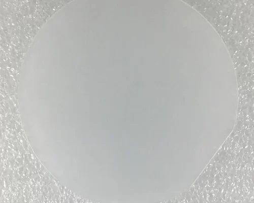
Product Overview
Sapphire (Al2O3) is the second-hardest material after diamond (Mohs 9), with the broadest optical transmission of any oxide (0.15-6.0µm), outstanding thermal/chemical stability (mp 2,040°C), and the most widely used substrate for GaN optoelectronics. C-plane is the industry-standard substrate for every blue/green/white LED globally. R-plane enables Silicon-on-Sapphire (SoS) RF ICs for military/space electronics. Princeton Powder supplies C/R/A/M-plane, 2″-8″, SSP/DSP CMP epi-ready (Ra<0.2nm).
Technical Specifications
| Parameter | Specification |
|---|---|
| Crystal Structure | Hexagonal (Rhombohedral), R3c; a≈4.77Å, c≈12.98Å |
| Purity / Density / Melting | >99.99% | 3.98 g/cm³ | 2,040°C |
| Hardness / Transmission | Mohs 9 | 0.15–6.0 µm (DSP T~86% uncoated) |
| Thermal Cond. / Expansion | ~40-46 W/m·K | ∥c: 6.66, ⊥c: 5.0 ×10⁻⁶/°C |
| Dielectric ε / Loss | A-axis ~9.4; C-axis ~11.58 @300K | loss <2×10⁻⁵ @10GHz |
| Orientations | C-plane (0001) — GaN LED | R-plane (1-102) — SoS RF | A (11-20) | M (10-10) ±0.2-0.5° |
| Wafer Sizes | 2-8″; thickness 430-1300µm; SSP CMP Ra<0.2nm / DSP Ra<0.5nm |
| TTV/Bow/Warp | <15µm / <20µm / <25µm (4″ typical) |
Applications
GaN LED Epitaxy — C-Plane
C-plane sapphire is the dominant substrate for GaN-based LED manufacturing worldwide — billions of LEDs annually. Off-M orientation (0.2±0.1°) for MOCVD step-flow growth.
Silicon-on-Sapphire RF ICs — R-Plane
R-plane enables radiation-hard, high-frequency SoS RF ICs for military radar, satellite comms, and space electronics. Insulating sapphire = perfect device isolation.
UV-IR Optical Windows
Mohs 9 + 0.15-6.0µm transmission = the definitive material for scratch-resistant spectroscopy windows, smartphone camera lens covers, and armored vehicle vision blocks.
FAQ
C-plane vs R-plane?
C-plane: GaN LED/laser epitaxy, optical windows. R-plane: Silicon-on-Sapphire RF ICs, non-polar GaN epitaxy. A/M-plane: specialized non-polar epitaxy research.
Sapphire vs SiC for GaN LEDs?
SiC: better lattice match (~3.4% vs 16%), 10× thermal conductivity — but sapphire is ~10× cheaper, larger diameters (8″ vs 6″), fully mature buffer layer process. >95% of commercial LEDs use sapphire.
DSP vs SSP?
SSP: front CMP epi-ready, back ground — for epitaxy. Lower cost. DSP: both sides polished (T~86%) — required for optical windows/transmission applications.